The Leading Printed Circuit Board Manufacturer and PCB Assembly -Shinelink Technology Ltd
We Offer a Full Range of Printed Circuit Board, PCB Capabilities to
Fit All of Your PCB Needs.
Shinelink Technology Ltd founded in the year 2005, located in Shenzhen,China. is an expert
at PCB manufacturer and PCBA manufactur, based in Shenzhen,
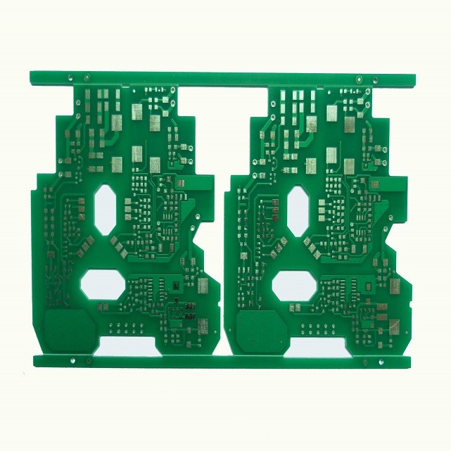
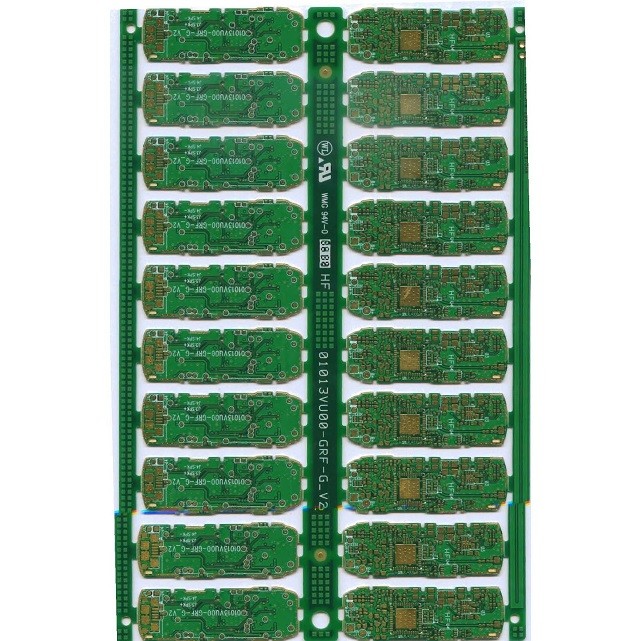
Guangdong, China. We are specialized in manufacturing Single-Sided
Boards, Double-Sided Boards and multilayer PCB, up to 20 layers.
also could provide components purchase and turnkey pcb assembly
service.
With more than A decade in the field of PCB prototype and
fabrication, we are committed to meeting the needs of our customers
from different industries in terms of quality, delivery,
cost-effectiveness and any other demanding requests. As one of the
most experienced PCB manufacturers in China, we pride ourselves to
be your best business partners of your PCB needs.
We are honored as the excellent supplier of many companies all
around this world. We can offer all kinds of services including PCB
manufacturing and PCB assembly sample orders and batch orders. For
pcb assembly, utilizing 8 high-speed SMT pcba lines from Yamaha and
Sony, to meet our customers' need.
One Stop Solution -- Beyond PCB Manufacturing
We have got the ISO9001:2000, ISO14001, UL and ROHS certifications.
Now our PCB daily capacity reaches 1000 square meters, and PCB
assembly can reach 100,000,0 units per month.
We deeply believe that our good service and experience will
completely meet you need. Integrity, value and innovation are the
forces that drive our success. We are the smart choice for you and
the trusted source at the center of your deal. Welcome the win-win
situation together.